
A high gain Transimpedance Amplifier for photodiodes
Introduction
The purpose of this article is to describe a simple design of a high gain transimpedance amplifier for photodiodes. Transimpedance amplifiers(TIAs) are commonly used to translate the current output of photodiodes and other sensors into a voltage. The most straightforward implementation of a TIA is with a feedback resistor from output to the inverting input of an operational amplifier. Although this circuit is very simple, it is still requires careful trade-offs among noise, gain and stability.
A generic opamp transimpedance amplifier (TIA) is shown below:

The detector is connected to the inverting input which is held at virtual ground due to the grounded non-inverting input. The photo-current flows through the feedback resistor 𝑅𝑓 leading to an output voltage equal to ≈−𝑅𝑓𝑖𝑝ℎ. 𝐶𝑓 provides compensation for the effects of the input node capacitance and stabilises the circuit.
The gain of the transimpedance amplifier is set by the feedback resistor; the higher the value of the resistance, the higher is the gain. However, this is at the expense of bandwidth. The feedback compensating capacitor also affects the bandwidth. Overcompensating the TIA, with a feedback capacitance larger than required to stabilise the TIA, will unnecessarily reduce the bandwidth.
A high gain TIA design while maintaining a wide bandwidth is achievable if the Gain-Bandwidth product of the operational amplifier is high. The OPA657 operational amplifier from Texas Instruments boast a 1.6 GHz gain-bandwidth product. Having a high 1.6-GHz gain bandwidth product gives greater than 10-MHz signal bandwidths up to gains of 160 V/V (44 dB).
High Gain Transimpedance Amplifier Schematic
The circuit was assembled with a feedback resistor of 200 kohms. The assembled PCB is also shown.


Circuit response
The frequency response of the TIA was measured using a network analyser with a 10 pF capacitance connected to the input to represent the junction capacitance of the photodiode.
With no feedback capacitance, peaking is clearly visible in the response. With a capacitance of 0.2 pF and 0.5 pF, a flat response is observed. With the 0.5 pF capacitance, the circuit is overcompensated, hence a reduced bandwidth is obtained.
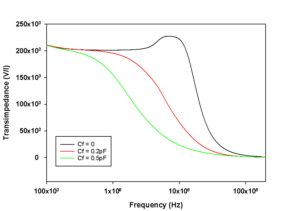
A reasonably high bandwidth and gain are obtained with minimal design, as shown in the frequency response.
Analytical Analysis
Consider the following figure, where the photodiode is represented by a current source Iph, a shunt resistor rs and a junction capacitor Cj

Using a first order model for the operational amplifier open loop gain given by:

..the transimpedance of the circuit (Vout/Iph) can be derived numerically and is equal to:

and the damping factor is equal to:

Using the following parameters, where A0 is the OPA657 DC open loop gain and τ0 is the time constant of the OPA657
cj := 10 pF; Rf := 200k; A0 := 3162; rs := 1G; τ0 := 0.89837e-6
The circuit frequency response can be obtained for different values of Cf:
With Cf := 0.1pF, a damping factor of ξ = 0.4366194372 is calculated and the numerical response looks like:

As observed with the measured response, the numerical frequency response also shows a clear peaking which will results in oscillations of the circuit output.
Increasing Cf to 0.2 pF reveals a flat response as expected:

The calculated damping factor ξ is 0.8499125050 which is above critical damping factor of 0.7071, hence gives a flat response.
If you have any comments or suggestions, contact us at [email protected]
Related Posts


About The Author
behindthesciences
We are two engineers who work in the Electronic and Telecommunication industry. We regularly blog in our spare time.
great work
I have question, in OPA657 datasheet noted:
“To reduce unwanted capacitance, a window around the signal I/O pins should be opened in all of the ground and power planes around those pins. Otherwise, ground and power planes should be unbroken elsewhere on the board ”
what does this meas, by window ? and also “”unbroken “”elsewhere ?
thanks guys
This just good practice when designing PCB. You need to design your ground and power plane properly in order to minimise parasitic capacitance, specially around you signal line.
Very informative and nicely written article!
I am currently building a transimpedance amplifier circuit for a photodiode using the Linear LTC6268-10 opamp which has a very high GBW of 4GHz. I am having trouble with persistent oscillation of the output signal, even with my feedpack capacitance an order of magnitude higher than the optimal value calculated for a 45deg phase margin. Is it possible for overcompensation to cause instability? Are there other possible causes of instability? I’d really appreciate a hint since I can’t figure out what’s wrong with my circuit.
Overcompensating will reduce the bandwidth but not instability. Instability can occur if your capacitance at the input is too high (including the photodiode capacitance); basically meaning that even if you think that you are overcompensating, you might not be.
Another reason could be that the capacitance at the output is too high to be driven by the LTC.